The laboratory is equipped with a cleanroom for the realization of devices for nano and micro (opto) - electronics, micro electro mechanical systems (MEMS / MOEMS) and microfluidics. Currently the complete line of process is possible on 3” wafers but there is the possibility to work, for some processes, on larger or smaller or uneven substrates. In general, the present apparatus allows to realize:
- nano and micro electronics devices on active structures of III-V materials or on substrates of different nature such as silicon, alumina, sapphire, glass or flexible substrates such as Kapton and PDMS;
- bulk and surface micromachining of silicon and SiC and organic materials (PDMS);
The areas certified in class ISO5, ISO6 and ISO7 total more than 150m2 to which about 100 m2 of grey areas are added. Inside the cleanroom, a staff of 6 units normally operates, and other 6 units are part time.
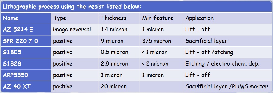
Optical lithography bay
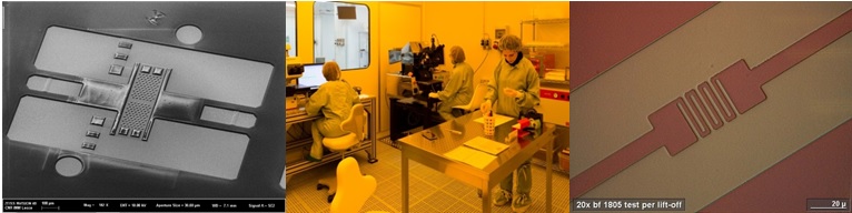
It contains all the necessary equipment for photolithography and cleaning of the samples (room size: 25m2 class : ISO 5).
- 1 semiautomatic maskaligner MA6 (Suss): any type of substrate – 4”, 3”, 2”, small pieces - 350W Hg lamp; UV: 365nm - front/back alignment option - motorized top side alignment system (alignment accuracy of ± 0.5 μm); 1 μm bottom side alignment accuracy;
- 1 semiautomatic spinner DELTA 80T (Suss): provided with gyrset to obtain uniform coating thickness on irregular substrates or with dense resist - Hot plates are used for resist baking. The spinner is used also for the deposition of e- beam resist and for the deposition of self-assembly nanoparticles ;
- 2 wet bench equipped with DI H2O, nitrogen. Used for sample cleaning, resist treatment
Nanolithography bay
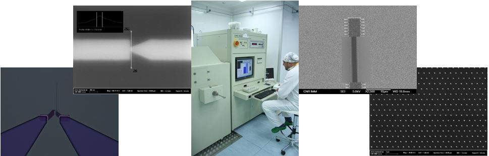
It contains the necessary equipment for e-beam lithography and a wet bench for chemical processes (room size: 25m2 class : ISO 6)
- 1 EBL CABL 9000C Crestec: Thermal field emission 5 - 50kV; field size modulation technology, minimum e-beam diam <2nm, minimum line width 10nm, stitching accuracy 50 – 10 nm, overlay accuracy 50 – 20 nm; 6”, 4”, 3”, 2”, small pieces substrates; pitching and overlay control (error <10 nm) on 4” wafer
- 2 wet benches equipped with DI H2O, nitrogen used for electron beam resist treatment and wet chemical etching; Hot plates used for resist baking.
Nanofabrication bay
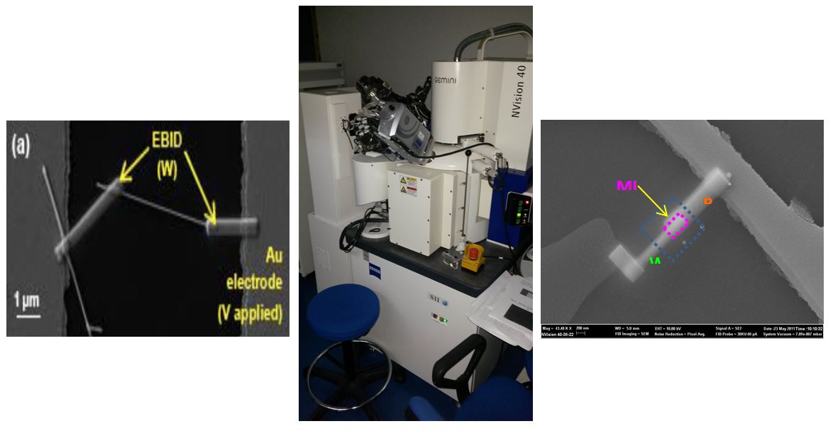
This laboratory, is not in inside the new cleanroom but it’s situated in the main Institute building.
- 1 FIB NVision 40 Zeiss: Cross-beam system integrating a high resolution (1 nm at 20 kV accelerating voltage) SEM GEMINI column and an ion column (30 keV Ga ions); Gas Injection System for electron- and ion- assisted deposition of metal and insulating layers; OXFORD INCA X-Act energy dispersive x-ray spectrometer.
Physical Deposition bay
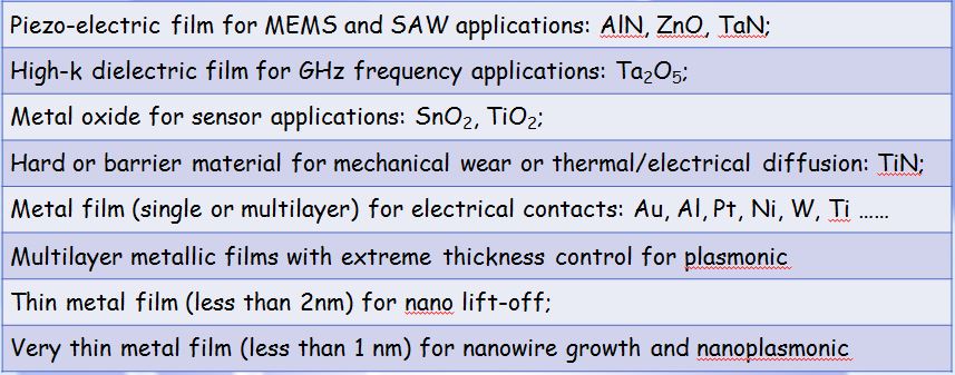
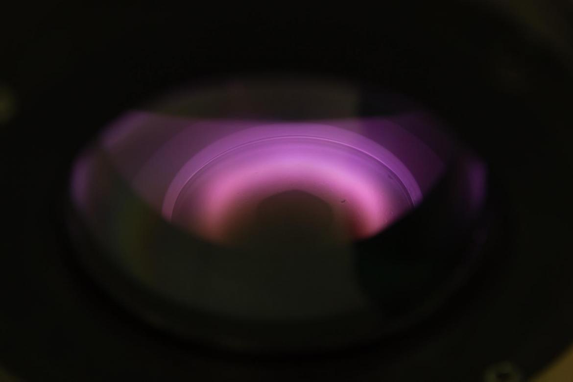
- 1 Sputtering SP404 IONVAC: Semi automatic system with load lock chamber; 4 targets 4” diameter; 2 RF (600W) 2DC (1kW); 3 gas sputtering Ar, N2, O2 (option for H2); substrate can be polarized (in-site cleaning and assistance) and controlled in temperature (up to 300°C); possible co sputtering (1DC-1RF or 2RF)
- 1 Thermal Evaporator: e-beam source: Caburn 4 crucible (6cc) 3KW source; beam sweep; thermal source: 4 liners (2KW); sequential deposition up to 8 different material; control of rate and thickness; rotable substrate;