The materials and devices characterization activity represents one of the main research activity of the IMM UNIT of Lecce. It involves a total of 9 researchers and 3 technicians and is carried out in 2 large laboratories, strictly interacting among them: the morphological and structural characterization laboratory, the optical and magneto-plasmonic characterization laboratory and the electrical characterization laboratory. The latter is a recent joint IMM-Nanotec facility (ELPHO), devoted to electrical and photoelectrical characterizations, which provides the study of charge carrier transport and device testing with high degree of flexibility.
Due to its transversality, the characterization activity is carried out in synergy with the various technological and application areas in which the unit is involved, but it is also dedicated to the development of new methodologies and to the implementation of unconventional and not commercially available experimental setup.
The optical and magneto-plasmonic characterization laboratory (R.Rella, M.Lomascolo, M.Manera, A.Cretì, G.Montagna)
In this laboratory, the following techniques and methodologies are available:
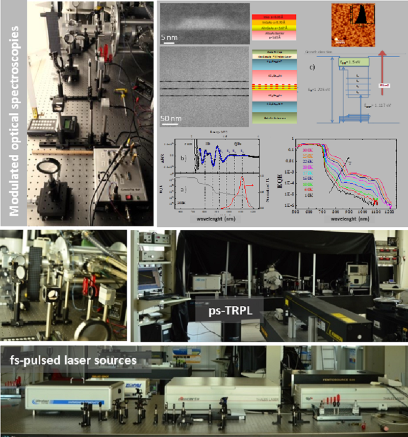
a) CW and ps-ns Time Resolved PhotoLuminescence in the UV-Vis-NIR spectral range. Sample temperature range 10-800 K. (M.Lomascolo, A.Cretì)
b) CW Modulated spectroscopy techniques such as Photo/Electro-Reflectance in the Vis-NIR spectral range, at single and double frequencies for background-free signal detection. Sample temperature range 10-800 K.(M.Lomascolo, A.Cretì)
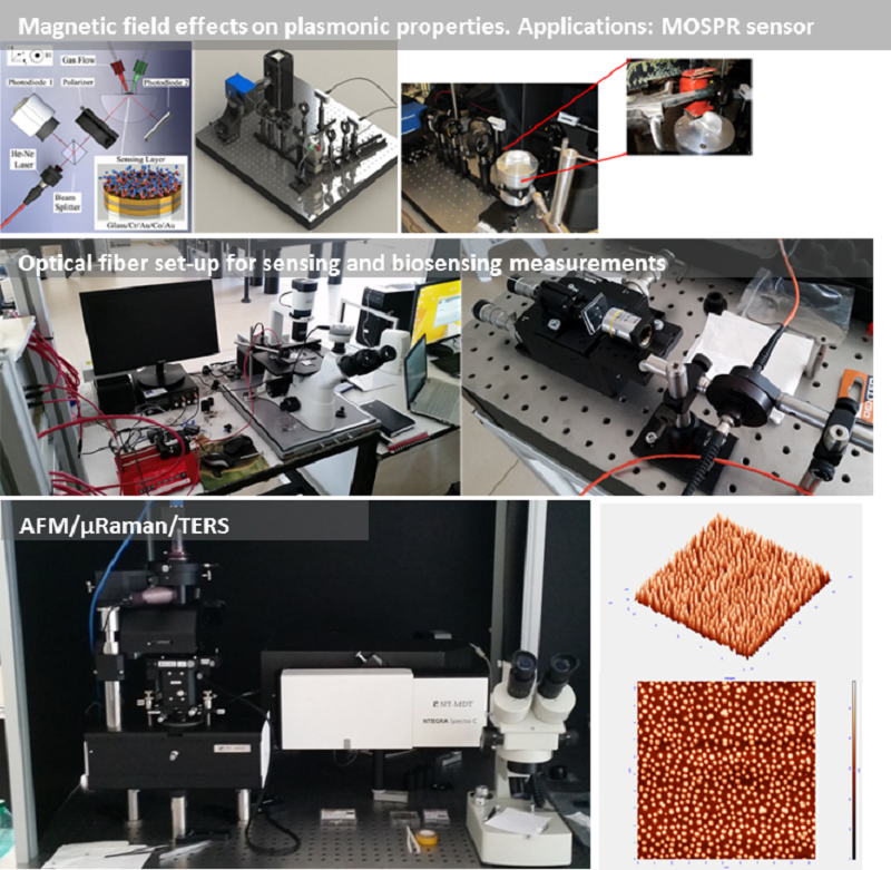
c) Surface and Localised Plasmonic (SPR, LSPR) characterization (Angular and wavelength modulation) (in Kretschmann configuration and fiber optical transmission/reflection set-ups). Magnetically-modulated SPR/LSPR setup in Kretschmann configuration (Angular and wavelength modulation). Both in controlled environment. (M. G. Manera)
d) Multichannel fiber-optics based LSPR setups for dynamic transmission/reflection and fluorescence characterization of nanostructured samples both in air and in liquid phase. (R. Rella)
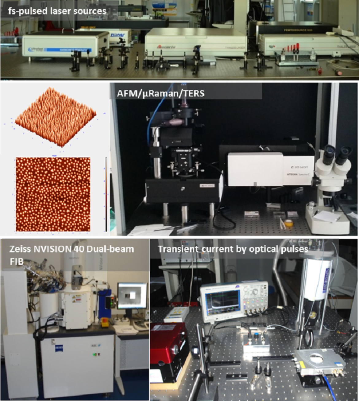
e) fs Pump and Probe transient spectroscopy (fs-T/T at 80 fs, 1.5 KHz, 1 mJ @810 nm). (M.Lomascolo,A.Cretì)
In the next, the Research activity will be focused on the implementation of:
a) Modulated Spectroscopy (UV-Vis-NIR) at single and double frequencies with meter spatial resolution, by means of microscope objective use.
b) Time-Resolved PhotoLuminescence spectroscopy (Vis-NIR) with meter spatial resolution by means of coupling of existent PL set-up with a confocal microscopy system.
c) fs Pump and Probe transient spectroscopy with meter spatial resolution by means of coupling of existent set-up with a confocal microscopy system.
Recently, multifunctional instrumentation for the opto/chemical characterization of the realized functional nanomaterials has been acquired; it allows: AFM/ microRaman spectroscopy and imaging, SERS and TERS spectroscopy and imaging, AFM/fluorescence microscopy, SNOM. (M. G. Manera)
The ELPHO (ELectrical and PHOto-electrical) laboratory (A.Cola, I. Farella, A.Persano, S.Gambino (Nanotec))
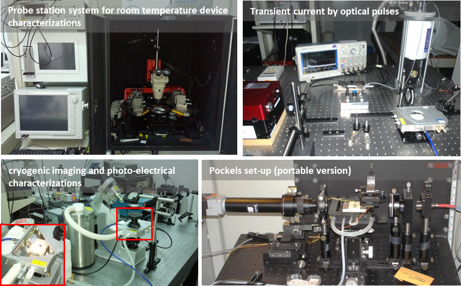
The wide range of investigated materials/device, their variable spatial scale, and their functionalities has made it necessary to establish a laboratory characterized by a high degree of flexibility and by the implementation of advanced electrical, photo-electrical and electro-optical techniques. In this laboratory, basic material properties can be explored (defects, charge transport dynamics, interfaces,etc.), and reliable device testing is carried out with updated high-performing equipment. This is strength of ELPHO (ELectrical and PHOto-electrical laboratory), a joint IMM-NANOTEC laboratory born in 2016, which is presently configured as summarized below:
• Time of Flight (TOF) measurements to study the charge carrier dynamics including carrier mobility in low conducting materials (OPO, supercontinuum and laser diodes optical sources).
• Linearly Increasing Voltage (CELIV) for the investigation of the transport properties of both high and low conductive materials, often applied to organic devices.
• Electroluminescence imaging in the VIS and NIR spectral ranges, to investigate spectral and spatial properties of light emitting devices. thermal stage with VIS and NIR imaging.
• Thermally Stimulated Current (TSC) measurements for the study of traps from carrier thermal emission during thermal scans.
• Junction Spectroscopy, deep level transient spectroscopy based on optical excitation (O-DLTS) and the thermal analysis of capacitance and current transients
• Photocurrent mapping, to probe the spatial photo-response of materials/devices with micro-meter resolution and wavelength choice. Standard spectral photocurrent (responsivity) set-up is also available.
• Hall effect, I-V, C-V-f, standard dc characterizations in probe station, cryostats (N2 Oxford, Janis), thermal stages. Keithley and Agilent Modular source-monitor-unit systems are present.
• Pockels effect, to study the electric field spatial and temporal behaviour inside field-induced birefringent materials like CdTe, GaAs etc. Thermal stage for measurements up to 400°CHall effect, I-V, C-V-f, standard dc characterizations in probe station, cryostats (N2 Oxford, Janis), thermal stages. Keithley and Agilent Modular source-monitor-unit systems are present.
• Pockels effect, to study the electric field spatial and temporal behaviour inside field-induced birefringent materials like CdTe, GaAs etc. Thermal stage for measurements up to 400°C
• Ionic mobility is measured in polymer films in lateral/vertical configuration by means of current/optical transmission transient measurements.
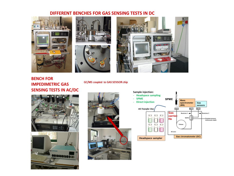
The electrical-functional characterization laboratory (S. Capone)
In this laboratory, the following techniques and methodologies are available:
a) DC Electrical-functional characterization for chemical sensing under controlled environment (automatized lab benches controlling signal acquiring, flow, analyte concentration, humidity, temperature, headspace sampling, breath sampling)
b) I-V characterization for chemical sensing under controlled environment
c) Electrical and Electrochemical Impedance Spectroscopy (EIS) under controlled environment for chemical sensing, investigation of semiconductor interface, analysis of dielectric material properties, electrochemical systems.
d) Chemical analytical methods by a peculiar configuration of a gas chromatograph (GC) coupled to mass spectrometer (MS) and gas sensor (GC/[MS+sensor] system) by a splitter for advanced analysis of different matrices in support to chemical sensing in environmental, medical, industrial and food application areas.
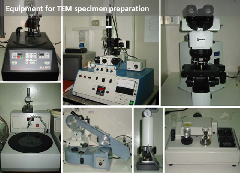
The morphological and structural characterization laboratory (Massimo Catalano, Antonietta Taurino, Antonio Pinna, Maurizio Russo)
This laboratory includes the following instrumentations:
a) a sample preparation laboratory, fully equipped for the conventional preparation of thin sections for transmission electron microscopy
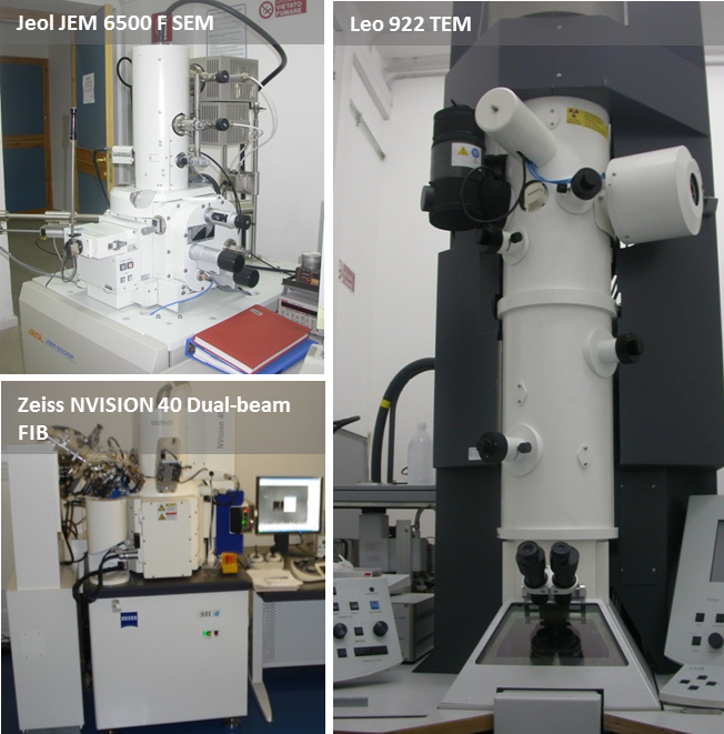
b) An NVISION40 Cross-Beam Focused Ion Beam (FIB) system, integrating a field emission Ga ion column and a high resolution Gemini FEG SEM column. The system is also equipped with:
- a Gas Injection System for electron and ion beam assisted deposition of Pt, W and SiO2 materials
- an Oxford 350 x-act energy dispersive x-ray spectrometer for chemical analysis.
This system has been used for:
- morphological characterization of surfaces and deep layers by in-situ preparation of cross-sections
- nanocontacting of single nanostructures
- hole nanopatterning of large areas (hundreds of square um) by single beam pixel exposure method
- nanocut (width of few tens of nm) on electrical contacts for trapping and measuring currents through single nanostructures
c) A Leo 922 Transmission Electron Microscope, operating at 200 kV, equipped with a built-in omega filter for electron energy loss spectroscopy (EELS), devoted to the conventional morphological–chemical characterization different type of materials.
d) A Jeol JEM 6500F Scanning Electron Microscope, located in the clean room, used for inspections of the results of clean room processes.