
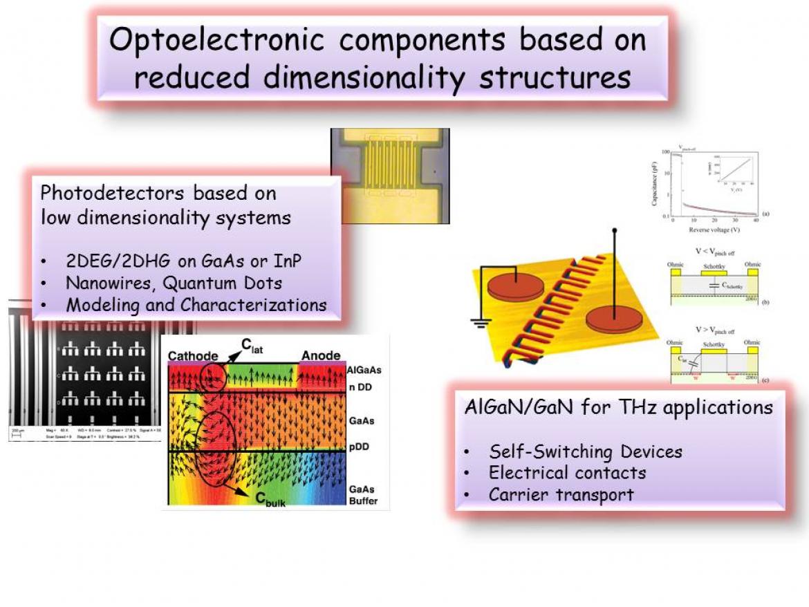
- Development of high-speed NIR photodetectors based on AlGaAs/GaAs heterostructures containing two dimensional (2D) charges
Metal-semiconductor-metal (MSM) photodetectors based on AlGaAs/GaAs heterostructures are developed. The presence of 2D allows to overcome the speed limits imposed by the carrier transit time: charge plasma confined in a semiconductor can transfer energy, hence respond much faster than the field induced carrier drift current. The activity is carried out on different structures, by studying the influence of [ref,ref, ref]:
- Bragg reflectors
- d- vs. uniform doping
- The two dimension charge gas, i.e. 2-DEG, 2DHG, 2DEHG [ref, ref, ref]
- active material (InGaAs, GaAs)
- material properties (growth Temperature) [ref]
Different Devices have been fabricated:
- Schottky interdigitated photodetectors
- Interdigitated detectors base on heterodimensional contacts (3D contact- 2D charge gas)
- HEMT
- Varactors [ref, ref, ref,ref]
Planar devices embedded in Transmission Lines for Electro-Optic time response studies are fabricated;
The activity has been extended to AlGaAs/GaAs Nanowires [ref], InGaAs Quantum Dots [ref, ref] , which exhibit a favorable photo-response, not only in terms of speed, but also sensitivity, noise and power consumption. Carrier transport is studied on single Nanowires (local absorption, response to polarized light, etc.) [ref] contacted by EBID (electron beam induced deposition) [ref]
The modeling activity is in collaboration with Drexel University (Philiadelphia) , while the electro-optic time response is carried out at NRL (Washington dc). The group in Lecce is mainly in charge of device fabrication and their characterizations.
2. Development of AlGaN/GaN devices for THz applications: The present activity is focused on the optimization of the ohmic contacts on AlGaN/GaN. This is a key-process for high power/high frequency applications and it is currently under way to enable the fabrication of nanometric THz emitters/detectors based on self-switching-devices (SSDs).
This activity is also supported by studies of carrier transport in AlGaN/GaN structures.
Beside the standard characterization tools, photocurrent mapping under suitable UV excitation wavelengths is implemented
This is an activity in collaboration with Montpellier University which is in charge of the device modeling and the THz characterization, and with Finmeccanica with regard to the ohmic contact optimization.