
1) Hetero- and nano-structures based on III-V (GaAs/AlGaAs) and II-VI (CdTe) semiconductors, such as nano-islands and dense vertical arrays of nanowires grown by self-assembly processes and selective area epitaxy have been the subject of intense recent examination due to their useful optical properties, such as enhanced light absorption which makes them effective substrates for solar cells
The 1D structure allows a more efficient light harvesting due both to the increased optical absorption related to the nanowire band structure and to the light trapping among the wires. Importantly NWs can occupy a fraction, about 10% of volume compared to bulk, can absorb an order of magnitude more light compared to thin films of the same height. Additionally the transport and collection of photogenerated carriers inside the core results greatly increased.
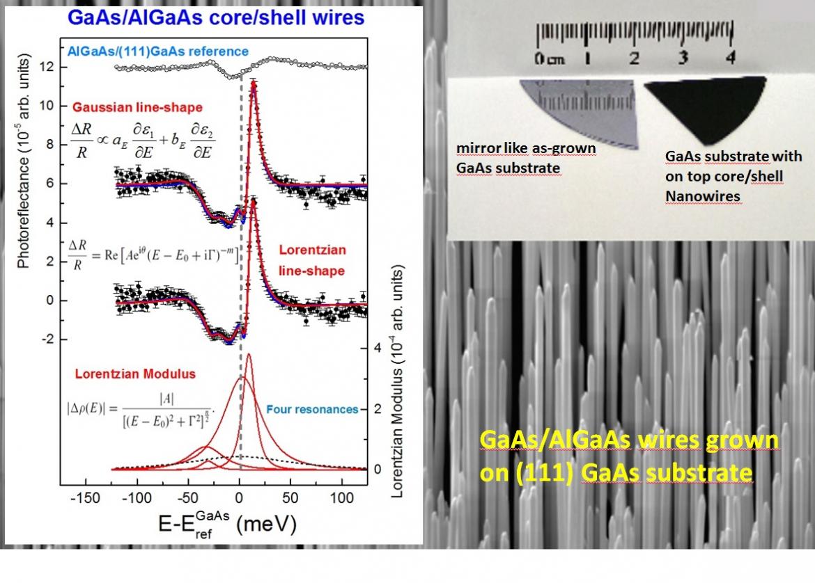
High-spectrally resolved room temperature photo-reflectance experiments in conjunction with Gaussian and Lorentzian line-shape ananlysis evidenced: a) fine structure optical transitions around the QW bandgap; b) an enhancement of the optical absorption in these nanowires systems of more than one order of magnitude if compared with the reference AlGaAs/GaAs thin films.
Activity in collaboration with University of Salento, funded by:
1- Project Phashyn - Reti di Laboratori-Regione Puglia: III generation photovoltaic based on nanowires (for GaAs/AlGaAs core/shell nanowires)
2- INNOVASOL”, PON MIUR: Development of innovative solar concentration technologies (for CdTe nanowires)
A. Cretì, M. Lomascolo (electro-optical characterization), P. Prete (Growth)
2) epitaxial hetero-structures (van der Waals epitaxy) of 2-dimensional (‘layered’) materials, such as graphene and graphene-like materials (TMDC and hexagonal boron nitride, h-BN) in collaboration with University of Salento.