
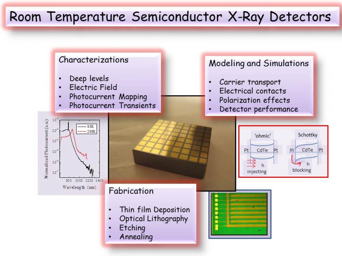
The Lecce IMM unit has a 20 years old research experience on room temperature semiconductors X-Ray Detectors. Past projects have been devoted to the development of GaAs and Cd(Zn)Te detectors for medical and astrophysical applications. Present activity is mainly focused on Modeling and simulations, Characterizations, and, to a minor extent, to Fabrication. An updated list of pubblications can be found here.
Modeling and Simulation
|
The modeling activity includes carrier transport mechanisms and the influence of defects and electrical contacts on the electrical properties of the detectors. For example, in semi-insulating GaAs, the mechanism of field-enhanced capture cross-section of the EL2 deep level has been clarified, including the consequences on the internal electric field distribution. For CdTe, a compensation model has been proposed and validated by the complementary analysis of both bulk and detector electrical properties. |
|
Numerical simulations of the electrical and detector properties are carried out by home-made or commercial (Synopsys) packages, in collaboration with IMM-Rome. In order to describe stochastic processes, like charge trapping or electron/hole pair photogeneration, the MonteCarlo method is applied. |
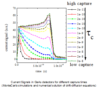
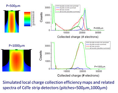
Examples of detector-oriented studies include the small pixel effect in GaAs detectors, irradiation angle on planar/strip CdTe detectors, optimization of the strip size, bias- and radiation-induced polarization, induced signals in GaAs detectors.
Characterizations
A large variety of electrical, photo-electrical, and electro-optical techniques are used to characterize the X-Ray detectors and the materials they are made of. The techniques include either conventional dc device testing, deep level spectroscopies and less conventional implemented techniques, such as those based on the current transients induced by optical pulses, and on the Pockels effect to access the detector internal electric field distribution.
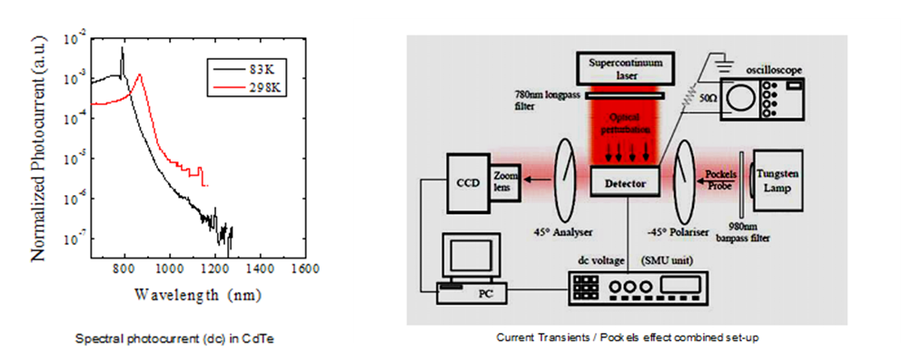
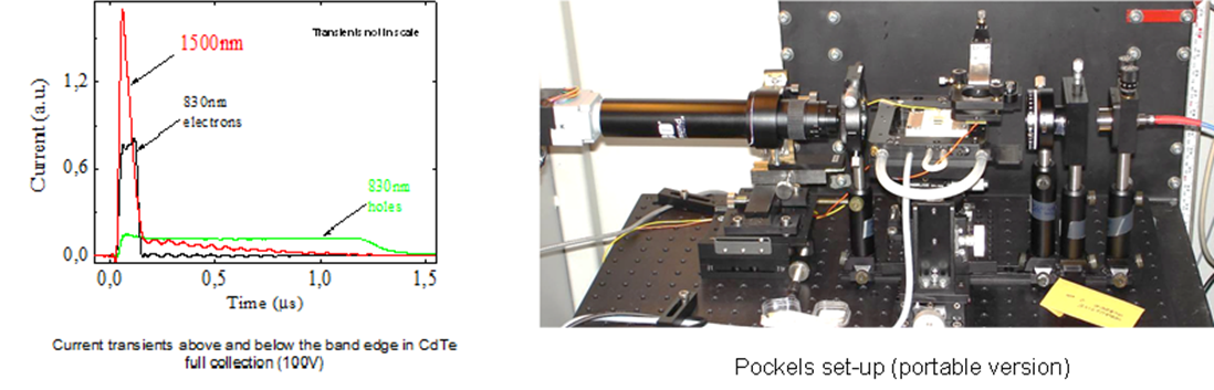
The measurements are carried out in the ELPHO (ELectrical and PHOtoelectrical) laboratory, a joint IMM-NANOTEC facility born in 2016.
Fabrication
|
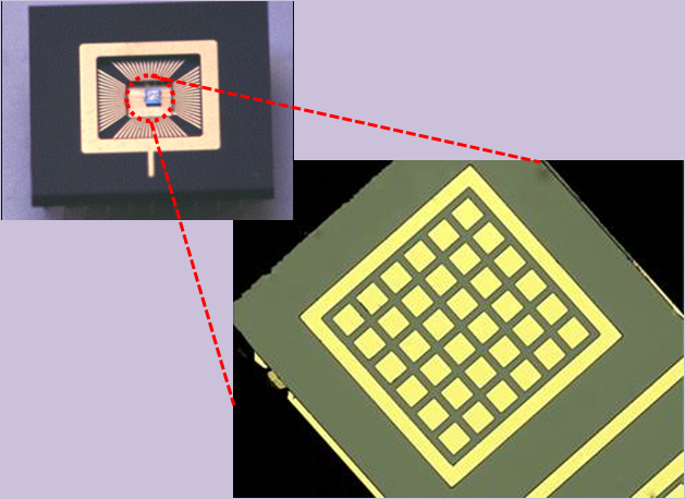
In the IMM clean-room facility (AMANDE lab) the basic processing steps for microelectronics can be performed. They have been applied to GaAs and CdTe (CdZnTe) bulk and epitaxial crystals to fabricate planar and segmented (strip, pixel) detectors with a great flexibility of electrode materials and architecture.
The processing steps include the depositions of Ohmic/Schottky contacts for GaAs and CdTe (CdZnTe) detectors; the dielectric/passivation layer deposition; the cleaning/etching processes by wet and dry (ICP, PECVD) methods; optical lithography and lift-off.
Annealing in controlled atmosphere are carried out either in conventional ovens and in rapid-thermal-annealing chamber. Galvanic and packaging (passivation, micro-bonding) processes are also used.
|